Highlights
Highlights
Simplifying Nanotechnology:The Development of a New Technique to Micropattern Carbon Nanotube Thin Films in One Step
- Read in Japanese
- 2014/05/08
 Dr. Yutaka Ohno, an associate professor at the Graduate School of Engineering, Nagoya University, and his co-researchers have successfully developed a new technique to transfer microscopic patterning of carbon nanotube (CNT) thin films onto plastic substrates in one step. Their paper was published online in ACS Nano on April 1, 2014.
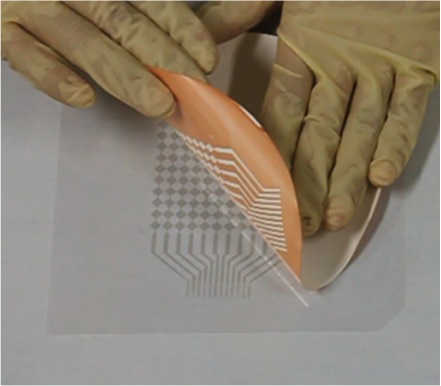
Transparent conductive films are essential components of various electronic devices such as displays and solar panels. Indium tin oxide (ITO) is widely used as a transparent conductive film. However, since ITO contains a rare metal, the cost and the sustainability of this approach are major concerns. Therefore, the development of an alternative film has been the subject of intense research. CNT thin films have recently attracted considerable attention and their practical use has started in touch panels and displays. Nevertheless, the conventional method for transferring the film onto a substrate requires numerous chemicals and expensive devices, and also involves a complex process. As a result, the development of a new and simple technique has been widely anticipated.
Prof. Ohno previously succeeded in producing flexible high performance carbon nanotube (CNT) integrated circuits on transparent substrates in 2011 and the world's first all-carbon integrated circuits in 2013, and has been leading the development of CNT thin-film formation technology worldwide. Recently, his research group has successfully developed a method to micropattern CNT thin films onto plastic substrates. This process simply involves collecting CNTs with a filter that forms a microscopic pattern and then transferring the pattern onto the plastic substrate. This novel technique has many advantages in that it can be conducted under normal atmospheric pressure at room temperature, the use of chemicals is reduced in comparison with previous methods, and 100% use of the CNT materials can be achieved. Furthermore, Prof. Ohno has used this technique to produce a touch sensor on a plastic substrate and has demonstrated multi-touch actions and the use of the substrate as a writing pad. This research will be practically applied to devices that require transparent conductive films, such as flexible touch panel devices, and will contribute to energy and resource savings and the reduction in CO2 emissions.
Associate Professor Yutaka Ohno
Prof. Ohno aims to create new electronics that can serve as important driving forces in Japanese industries. He believes that conventional electronics has already reached its ultimate performance capabilities. Therefore, he differentiates himself from researchers focused on conventional systems by adopting a new perspective based on physical phenomena (new functionalities) associated with nanostructure materials such as carbon nanotubes.
Outlook for the Future
"I would like to conduct research on the interactions between electronic devices and the human body and brain, and develop new electronic devices; for instance, one that is unrecognizable, fitting naturally into ambience, or one that is wearable with an affinity for the human body."
Message to Young Students
 "In engineering research, I find it particularly appealing that I can develop new technologies that no one has ever imagined and create a completely new substance. Although the physical properties of materials found in nature cannot be changed, innovative ideas can lead to new and more efficient uses of existing materials as well as the development of new substances. To achieve this goal, it is important to adopt a fine perspective by seeing things from different angles."
Links
Research Information
Nagoya University Press Release (Japanese)
ACS Nano
Associate Professor Yutaka Ohno Information
Ohno Group/Quantum Nanoelectronics Labo.
Nagoya University Faculty Member Profile